


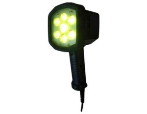
Wafer inspection: yellow LED lighting system for high-quality wafer testing
Yellow Wafer Semiconductor Inspection Lamps from SECU-CHEK
(Wafer Semicondutor Inspection Lamps SLEX-GB-H127-SFN-DNF)


Optical wafer inspection specially designed for quality assurance and testing of wafers
integration of the systems into existing reactors
Wafer surface inspection to increase ROI
Wafer inspection with yellowlight lamps / wafer surface inspection with greenlight lamps
- Wafer inspection with High-Tec yellow light lamp without UV radiation
- Replacement of UV lamps for inspection of wafers
- Testing of wafers without the use of mercury vapor lamps
- Designed as a filtered green light lamp or as a filtered yellow light lamp for wafer inspection
- Wafer surface inspection with SECU-CHEK wafer test lamps without UV and without mercury
Choose a robust, low-maintenance yellow light lamp for optical wafer inspection
with comprehensive process reliability thanks to extremely strong display of failures
and enormous energy savings compared to 100 watt mercury discharge bulbs


Why use filtered Yellow Light Lamps from SECU-CHEK for Wafer Surface Inspection?
- High process reliability required for wafer production
- economically efficient and trouble-free test operation desired
- a solid wafer test is crucial for the further cost-intensive steps of wafer preparation and chip production
- Professional solution according to industry standard required
Request now price for the wafer Semicondutor Inspection Lamp SLEX-GB-H127-SFN-DNF from SECU-CHEK!


What are the errors in wafer production and how well are they recognizable with the SECU-CHEK yellow light lamp?
- Faults of the wafer are well detectable with the filtered yellow light lamp
- Detect inclusions with the wafer test
- Detect contaminations by visual wafer testing
- See growth disturbances with yellow-green light
- Identify veils during optical wafer test
- Analyze stripes with the SECU-CHEK wafer inspection lamp
- Detect microstructures better compared to UV lamps and mercury lamps for wafer testing
- Detect growth holes with wafer inspection
- Check the edge flattening with high contrast of the yellow-green lamp
- Edge interferences can be found with the optical wafer inspection
- Detect structural shifts with the quality inspector lamp on the wafer
- Detect inclusions in wafer production with UV yellow light and green light lamps
- Idendify unevenness with the filtered yellow light light
- Identify limited clarity through high-quality wafer inspection
Common questions when visually inspecting wafers with yellow light lamps
- What illumination and intensity do I need for reliable test results during wafer inspection?
- Where/How are the lamps integrated for surface testing of the wafers in order to enable efficient workflows?
- What are the mounting options and open spaces for the yellow light lamp in the laboratory area?
- Do the processes and safety mechanisms of the yellow light or green light lamp meet the requirements that we have to meet?
- Who takes care of the instruction for error detection during the wafer test?
- What maintenance and repair costs do I have to plan for the UV lamp for wafer testing?
The yellow light lamps and green light lamps from SECU-CHEK with the special LED technology is your solution that is perfectly adapted to your test situation. Request a yellow light lamp to test your wafers today!

Wafer Inspection Technology for Chip Manufacturing and Solar Manufacturing
Manual wafer testing with high-tech yellow light lamps
- strong, extremely uniform, low-shadow illumination at the required intensity
- many advantages over automated wafer inspection – reduce the reject rate
- optimal for visual post-inspection of sorted wafers during automatic wafer inspection
- Evaluation and testing of all types of wafers in wafer production
 Manual optical wafer testing
- Easy integration of visual inspection into the wafer manufacturing process
- all kinds of wafers in photovoltaics as well as silicon wafers and much more. More
- High flexibility in wafer inspection with high error detection rate
Yellow filter and green filter for perfect visual inspection
- robust yellow light lamp housing for continuous operation during wafer inspection
- easily replaceable filter disc for the wafer lamp
- UV wafer lamp optional with active fan cooling for particularly long service life
Improve wafer production with manual wafer inspection
- Yellow light lamp for wafer testing: emitted in an optimized wavelength range, including the wavelength of 546, 577 and 579 nm, typically emitted by inspection lamps based on mercury vapour discharge bulbs as peak wavelength
- yellow better than green (525 nm) for high-contrast detection
- no flickering during the wafer test
- dimmable yellow light lamp that can be used to adjust the intensity to the best level for all types of inspections and types of errors
- Inspection lamp for semiconductor wafers
- LED-based replacement for common yellow light lamps
Which types of wafers can be tested with the SECU-CHEK yellow light lamp?
 Wafer inspection in semiconductor and chip manufacturing
- Wafer testing for the solar industry and photovoltaics
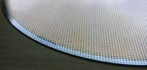
- visual wafer surface testing for all wafer sizes: 1-inch (25mm), 1,5-inch (38mm), 2-inch (51mm), 3-inch (75mm), 4-inch (100mm), 5-inch (125mm), 6-inch (150mm), 8-inch (200mm), 12-inch (300mm), 18-inch (450 mm)
- Inspection of epitaxed wafers
- optical testing of monocrystalline wafers and also polycrystalline wafers
- visual test of the surface of silicon wafers
- Check also possible for square wafers
- Testing of raw wafers and structured wafers
- Analysis of the surface of epitaxy wafers (EPI wafers) and SOI wafers
- Gold wafers test with the yellow light lamp
- Visual inspection with the UV lamp for crystalline silicone wafers
- Optical surface inspection for wafers of all materials: silicon, germanium, slicium carbide, gallium arsenide, sapphire, glass, etc.
- Visual inspection for SEMI standard wafers
- Quality check of bonded wafers, wafers on tape
- visual wafer inspection also for bare, thinned and fan-out wafers
- Optical quality control and inspection of strongly curved wafers (eLWB, etc.)
- etc.
 Wafer inspection in semiconductor and chip manufacturing
We look forward to your inquiry!
You are also welcome to contact us by phone or email.
Direct contact:
SECU-CHEK GmbH
An der Fähre 9
66271 Kleinblittersdorf
GERMANY
Phone +49 6805-942859-0
Fax +49 6805-942859-95
Email: info@secu-chek.de

By loading the map, you agree to Google's privacy policy.
Learn more
Wafer manufacturing - Knowledge and information
What is a wafer?
- Wafer stands for “thin biscuit” or “thin slice”
- a wafer is mostly circular, but partly also square
- the production of wafers is carried out from so-called ingots
- Wafers are usually a base plate for electronic components and elements
Use of wafers
- Chip production (integrated circuits)
- Microelectronics
- Photovoltaic (solar cells)
- Microsystem technology
More interesting information about wafer production and inspection
- Optical inspection solutions for highly integrated wafer testers
- Wafer inspection
- Inspection system for silicon wafers
- Automated wafer inspection
- Semiconductor Wafer Inspection
- Fully automated wafer inspection – YouTube
- Optical Wafer Inspection
- New measurement method for wafer inspection (article in german language)
Building a wafer
- Material: mostly silicon, partly also silicon carbide, gallium arsenide and indium phosphide
- partly also glass or gold wafers
- Size: 1 inch wafer to 18-inch wafer, with 18-inch wafers not yet possible for mass production
- there are various methods for the production of the ingots, e.B. the Czochralski process, etc.
Wafers in photovoltaics
- Differentiation of polycrystalline (multicrystalline) and monocrystalline wafers
- Wafers are produced by sawing the ingots
- square-shaped silicon blocks mostly for solar cell production
- round, monocrystalline wafers of cylindrical ingots mostly for chip manufacturing and microelectronics
More information about wafer production, wafer testing, etc. can be found here: Wikipedia
 Wafer inspection with Yellow lamps LED lighting system for high quality wafer testing
LED-technology for wafer inspection and wafer production. Our research has shown that we can better understand the internal characteristics of a material while maintaining its optical performance, as well to predict which materials will be suitable for certain applications. This leads us towards our next step: manufacturing specific components using only this technology! The company offers laser cutting capabilities in several types – from carbon fiber laminated molds and solid state coolants, through custom designed parts like flashlights and thermal control panels.
Wafer inspection with Yellow lamps LED lighting system for high quality wafer testing
LED-technology for wafer inspection and wafer production. The company has a long history in creating innovative products designed to meet the highest standards of safety, product performance designability as well cost efficiency while providing professional services that are applicable to large enterprises and industries worldwide through its facilities within Europe. We provide comprehensive Wafer Inspection service offered by experienced certified professionals within our European Headquarter.
Explore how the Wafer production process is organized and which tools you need to make a good wafer inspection. , we give tips on everything from making sure your scanner has all the necessary features before cutting it up to troubleshooting bad prints by learning about mistakes made with one of our most common items.
Silicon Wafer Production Process
Semiconductors are extremely critical and central components in modern technology. Most of the electronic devices we use today operate on these integrated circuits that are housed on silicon wafer chips. It does, however, take a lot of processing and work to get the semiconductor in that condition from the raw material. The basic substrate of these microchips is the silicon wafer chip upon which all the microfabrication takes place.
In this article, we will take a detailed look at just what constitutes the silicon wafer production process.
What are Silicon Wafers?
To begin with, we have to acknowledge that semiconductor wafers are made out of silicon- an element that makes up almost 30% of the Earth’s crust. It is the raw material that constitutes the basic structure of the whole semiconductor chip and is responsible for its optimum functioning. Rather than being a very good conductor of electricity, silicon has the property to control resistivity based on dopants. This silicon material has to be turned into a wafer before a semiconductor can be built on it. This means that the entire fabrication process to create the rest of the integrated circuit that will ultimately be a component of a larger electronic device rests on this tiny piece of a pure, crystal of silicon wafer.
The Silicon Wafer Production Process
 Following are the steps involved in ultimately producing a silicon wafer which then undergoes even more process to be turned into a semiconductor:
Ingot Growth
The very first step in silicon wafer production is to grow a nugget of silicon, also referred to as a silicon ingot. Growing a single silicon ingot can take as less as one week to up to one month. The time taken for the ingot growth is determined by the size, quality, and the specification of the wafer. One of the most common methods used to grow the crystal is the Czochralski Method or the CZ Method. Another method is the Float Zone technique, but it is seldom used in the current practice. In the former method, polycrystalline silicon pieces are put in a trough made of quartz. Small quantities of dopants are added which are basically elements from Group 3 and 4 of the periodic table, such as Boron, Phosphorus, Arsenic, or Antimony. These dopants are responsible for determining the properties of the resultant wafer material- it may be P type (Boron) or N type (Phosphorous, Arsenic, Antimony). The material is then heated above a temperature of 1412 degrees (usually above 1500 degrees) until everything has liquefied.
Then, a silicon crystal having the same orientation as the intended end result of the process is placed inside as a seed to facilitate the growth of the crystal with minimum defects. Once we reach the required diameter of the crystal, the process is stopped by stabilizing the conditions.The resulting material is referred to as electronic grade silicon to EGS. This silicon ingot can subsequently be used to cut and molded into the shape needed for the final silicon wafers for the semiconductor.
Slicing
The end diameter of the grown ingot is usually kept a little bit larger than what is actually required. As a result, we need to slice the wafer after it has been adequately inspected. A diamond edge saw is used for this purpose to make the wafer thinner and smaller without causing any major damage.
Lapping
The next step once the wafers have been sliced is lapping. Lapping refers to when the marks and defects left behind because of the sawing and other surface abrasions are removed. This step also serves to thin out the wafer a bit more as well as relieve the stress that the wafer has undergone during the slicing process.
Cleaning
Once we are done with lapping, the wafers must be chemically etched and cleaned. This further helps to alleviate any cracks or surface defects that may still be there, even on a microscopic level. This is usually done using a bath consisting of sodium hydroxide, acetic acid, or nitric acid.
Polishing
Finally, the wafer has to be polished to reach its final stage. This is performed in a clean room where the particle quantity per cubic foot is controlled to be somewhere between Class 1 to Class 10,000. Workers have to wear clean suits, work under a fan that blows away excess particles, and maintain a level of cleanliness on their workstations. High quality silicon wafers usually go through two to three stages of polishing. Wafers can either be single side polished or double side polished, with most only polished on the front. The polishing process itself has two stages- the first being the stock removal process which removes a thin layer of silicon to make sure the surface does not have any defects. The second part is the chemical mechanical polish which does not remove any silicon layers, but instead gives it a shiny, mirror finish.
Packaging
Once the silicon wafers are all nice and polished, they undergo a series of baths for proper cleaning and are inspected multiple times under high intensity lights to ensure there are no excess materials or defects on the wafer surface. After the cleaning and inspection is done, the wafers that meet the specifications and are in top shape are packed and sealed to be shipped out to the respective places in vacuum sealed plastic bags to keep the moisture out and prevent any damage during storage and travel before they are ultimately put to use as semiconductor substrates.